
CD4081 IC
497 in stock
Quick Overview:
- Features High Speed (tpd 10-50ns)
- Data rate (Max) (Mbps) 8
- IOL (Max) (mA) 6.8
- IOH (Max) (mA) -6.8
5.00 SAR
497 in stock
CD4081 IC
AND gates, provide the system designer with direct implementation of the AND function and supplement the existing family of CMOS gates.
The CD4081 types are supplied in 14-lead hermetic dual-in-line ceramic packages (F3A suffix), 14-lead dual-in-line plastic packages (E suffix), 14-lead small-outline packages (M, MT, M96, and NSR suffixes), and 14-lead thin shrink small-outline packages (PW and PWR suffixes).
Features:
Medium-Speed Operation – tPLH, tPHL = 60 ns (typ.) at VDD = 10 V
100% tested for quiescent current at 20 V
Maximum input current of 1 µA at 18 V over full package-temperature range: 100 nA at 18 V and 25°C
Noise margin (full package-temperature range) =
1 V at VDD = 5 V
2 V at VDD = 10 V
2.5 V at VDD = 15 V
Standardized, symmetrical output characteristics
5-V, 10-V, and 15-V parametric ratings
Meets all requirements of JEDEC Tentative Standard No. 13B, “Standard Specifications for Description of ‘B’ Series CMOS Devices”
Specifications:
Parameter Specification
Part number CD4081B
Technology Family CD4000
VCC (Min) (V) 3
VCC (Max) (V) 18
Channels (#) 4
Inputs per channel 2
Input type Standard CMOS
Output type Push-Pull
Features High Speed (tpd 10-50ns)
Data rate (Max) (Mbps) 8
IOL (Max) (mA) 6.8
IOH (Max) (mA) -6.8
Package size: mm2:W x L (PKG) 14PDIP: 181 mm2: 9.4 x 19.3 (PDIP|14)
Rating See Data Sheet
Operating temperature range (C) -55 to 125
Package Group PDIP|14
Related products
-
Integrated Circuits, Motors & Drivers, All Products
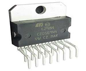
L298N Multiwatt-15V Dual Full-Bridge Driver
QUICK OVERVIEW
- Low saturation voltage
- Over temperature protection
- High noise immunity
- Applications: Motor Drive & Control
- Operating Supply Voltage Up To 46 V
- Total Dc Current Up To 4 A
- Low Saturation Voltage
- Overtemperature Protection
SKU: AC178

Reviews
There are no reviews yet