

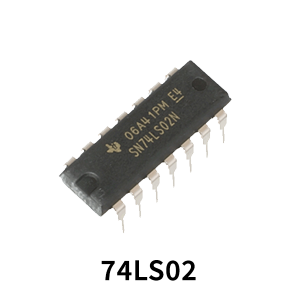
74LS08 AND gate
157 in stock
Quick Overview:
- Operating voltage range: +4.75 to +5.25V
- Recommended operating voltage: +5V
- Maximum supply voltage:7V
- Maximum current allowed to draw through each gate output: 8mA
5.00 SAR
157 in stock
74LS08 IC
is a member of 74XXYY IC series. There are four AND gates in the chip and each gate have two inputs, hence the name QUADRUPLE 2- INPUT AND GATE. The gates in the chip are designed by SCHOTTKY TRANSISTORS for high speed logic operations.
74LS08 Pin configuration
74LS08 is a 14 PIN IC. The chip is available in different packages and is chosen depending on requirement. The description for each pin is given below.
Features and Specifications:
- Operating voltage range: +4.75 to +5.25V
- Recommended operating voltage: +5V
- Maximum supply voltage:7V
- Maximum current allowed to draw through each gate output: 8mA
- TTL outputs
- Low power consumption
- Typical Rise Time: 18ns
- Typical Fall Time: 18ns
- Operating temperature:0°C to 70°C
- Storage Temperature: -65°C to 150°C
74LS08 Equivalents
SN54LS08, IC 7408, HEF4081, Any two transistors can be reconfigured to form a AND gate.
Where to Use 74LS08 IC
There are many applications of IC 74LS08. A few mentioned below.
1. The chip is basically used where AND logic operation is needed. There are four AND gates in the chip, we can use one or all gates simultaneously.
2. The chip is used in systems where high speed AND operation is needed. As mentioned earlier the gates in the chip are designed by SCHOTTKY TRANSISTORS to make the switching delays of gates less. Because of this the chip can be used for high speed AND operations.
3. 74LS08 is one of cheapest IC present in market for AND logic operation. It is really popular and is available everywhere.
4. The chip provides TTL outputs which are needed in some systems.
8 reviews for 74LS08 AND gate
Related products
-
Integrated Circuits, All Products
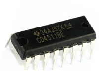
CMOS IC 4511 CD4511BE CD4511 DIP-16
QUICK OVERVIEW
- High-output sourcing capability up to 25mA
- Input latches for BCD Code Storage
- Lamp Test and Blanking capability
- 7-Segment outputs blanked for BCD input codes > 1001
- 100% tested for quiescent current at 20V
SKU: AC084 -


شيماء (verified owner) –
شيماء –
roaa (verified owner) –
I bought several of these
roaa –
Othman A. (verified owner) –
Othman A. –
منى ع. (verified owner) –
منى ع. –
Ahmad Fakhouri (verified owner) –
Ahmad Fakhouri –
Abdusalam Alhomidi (verified owner) –
Abdusalam Alhomidi –
سعود ا. (verified owner) –
سعود ا. –
King Khalid University Computer Sciences College (verified owner) –
King Khalid University Computer Sciences College –